Microstrip or patch antennas are becoming increasingly useful because they can be printed directly onto a circuit board. Microstrip antennas are becoming very widespread within the mobile phone market. Patch antennas are low cost, have a low profile and are easily fabricated.
Consider the microstrip antenna shown in Figure 1, fed by a microstrip transmission line. The patch antenna, microstrip transmission line and ground plane are made of high conductivity metal (typically copper). The patch is of length L, width W, and sitting on top of a substrate (some dielectric circuit board) of thickness h with permittivity
 . The thickness of the ground plane or of the microstrip is not critically important. Typically the height h is much smaller than the wavelength of operation, but not much smaller than 0.05 of a wavelength.
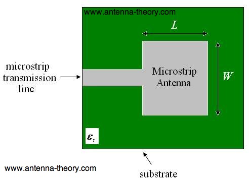 (a) Top View of Patch Antenna
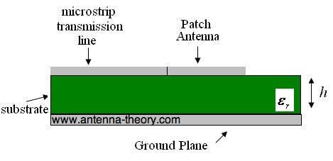
(b) Side View of Microstrip Antenna
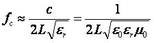
Figure 1. Geometry of Microstrip (Patch) Antenna.
The width W of the microstrip antenna controls the input impedance. Larger widths also can increase the bandwidth. For a square patch antenna fed in the manner above, the input impedance will be on the order of 300 Ohms. By increasing the width, the impedance can be reduced. However, to decrease the input impedance to 50 Ohms often requires a very wide patch antenna, which takes up a lot of valuable space. The width further controls the radiation pattern. The normalized radiation pattern is approximately given by:
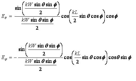
 . The magnitude of the fields, given by:
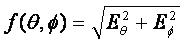
 .
.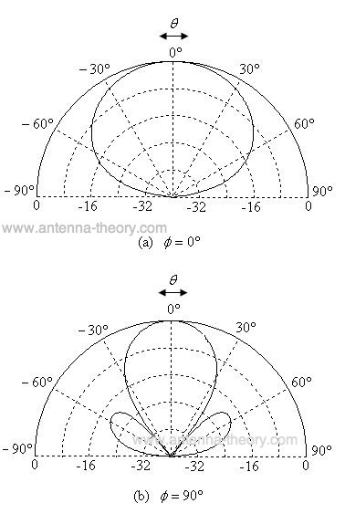 Figure 2. Normalized Radiation Pattern for Microstrip (Patch) Antenna.
Fringing Fields for Microstrip Antennas
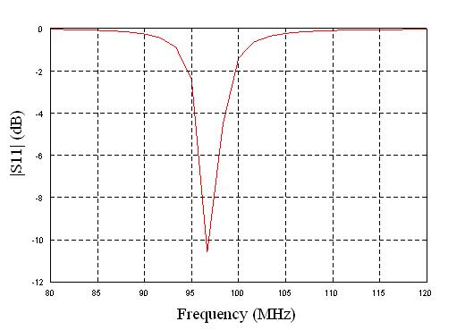 Figure 3. Magnitude of S11 versus Frequency for Square Patch Antenna.
Since the patch antenna can be viewed as an open circuited transmission line, the voltage reflection coefficient will be -1 (see the transmission line tutorial for more information). When this occurs, the voltage and current are out of phase. Hence, at the end of the patch the voltage is at a maximum (say +V volts). At the start of the patch antenna (a half-wavelength away), the voltage must be at minimum (-V Volts). Hence, the fields underneath the patch will resemble that of Figure 4, which roughly displays the fringing of the fields around the edges.
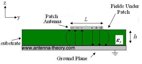 Figure 4. Side view of patch antenna with E-fields shown underneath.
As a side note, the smaller
is, the more "bowed" the fringing fields become; they extend farther away from the patch. Therefore, using a smaller permittivity for the substrate yields better radiation. In contrast, when making a microstrip transmission line (where no power is to be radiated), a high value of is desired, so that the fields are more tightly contained (less fringing), resulting in less radiation. This is one of the trade-offs in patch antenna design. There have been research papers written were distinct dielectrics (different permittivities) are used under the patch antenna and transmission line sections, to circumvent this issue.Next, we'll look at alternative methods of feeding the microstrip antenna (connecting the antenna to the receiver or transmitter).
source:http://www.antenna-theory.com/antennas/patches/antenna.php#introduction
No comments:
Post a Comment